Product introduction
The BJ8M601A is a single chip 8-bit MCU based on RISC architecture with built-in 2K×16-bit MTP program memory. It is manufactured using an advanced CMOS process withlow power consumption characteristics and low operating voltage capability. The chip integrates a multi-channel 12-bit A/D converter, as well as two timer modules that provide timing, counting and PWM functions. Internal watchdog, low voltage reset, low voltage detection functions ensure the reliable operation of the system. At the same time, it provides a rich clock options, including internal fast clock, internal slow clock, external crystal clock and external input clock, so that users can use flexibly. In addition, the MCU includes rich IO resources and can be widely used in various products.
Application field
Consumer electronics, small appliances, etc.
CPU characteristics
RISC architecture, 1T kernel.
8 layers of hardware stack.
Store
Program memory: 2K x 16bits.
Data RAM: 128 x 8bits.
Instruction set
68 instructions.
Interrupt
Unique interrupt entry address (08h).
8 interrupt source(T0/T1/INT0.1/LVD/ADC/PWM0.1).
I/O port
There are 14 I/O ports in total, and P12 provides input only.
All pins can be individually programmed.
8 pins have wake up function: P1.
14 pins have an internal pull-up function.
7 pins have an internal pull-down function: P1.
7 pins have open drain: P1.
2 external interrupts: P15 (external interrupt 1), P17(P01) (external interrupt 0).
2 pins have 40mA low drive capacity P03, P13.
Timer/counter
Timer/counter 0
8-bit basic timer/counter.
Supports the pre-division function.
Timer/counter 1
Automatic loading of 16-bit timer/counter.
2 PWM channels, support complementary output and dead zone can be matched.
Supports the pre-division function.
12-bit ADC
10 external input channels.
3 internal channels (internal reference voltage, internal VDD/4, internal GND).
AD Reference voltage: VDD, external reference voltage, internal reference voltage (2V,3V, 4V).
Watchdog timer
Supports the pre-division function.
Can configure overflow reset or wake up.
Clock system
Internal RC oscillator (master clock)
Frequency: 1MHz, 8MHz, 16MHz, error: ±1%.
Internal RC oscillator (WDT clock)
Frequency: 128KHz, error: ±3%.
External crystal oscillator can be configured
Supports 32768Hz to 16MHz external crystal oscillator.
Supports crystal and ceramic oscillators.
External RC oscillator
Frequency: 100KHz~10MHz, error: ±5%.
External clock source
Operating frequency: 32768Hz~16MHz.
Can work with dual clocks
Oscillator can be divided frequency: 1, 2, 4, 8.
Working mode
Common mode: Both high-speed and low-speed clocks work properly.
Low-speed mode: Only the low-speed clock works properly.
STOP mode: All clocks stop working.
IDLE mode: The CPU stops working and peripherals can work.
Low voltage reset (LVR)
Low voltage reset options: 1.8V, 2.3V, 2.7V, 3.0V, 3.3V, 3.6V, 3.9V.
Reset time: 140us, 6.5ms, 18ms, 72ms, 228ms.
Low Voltage Detection (LVD)
Low voltage detection options: 2.2V, 2.4V, 2.6V, 2.9V, 3.2V, 3.8V, 4.1V.
Can be configured to generate interrupts.
Low power mode
The power consumption in STOP mode is less than 1.2uA.
I/O, level trigger mode for external interrupts, RTC mode for timer 0, and watchdog wakeup.
Operating temperature range
-40℃ ~ +85℃.
Voltage operating range
2.0V~5.5V.
Anti-interference capability
ESD: Better than ±4000V.
EFT: better than ±4000V
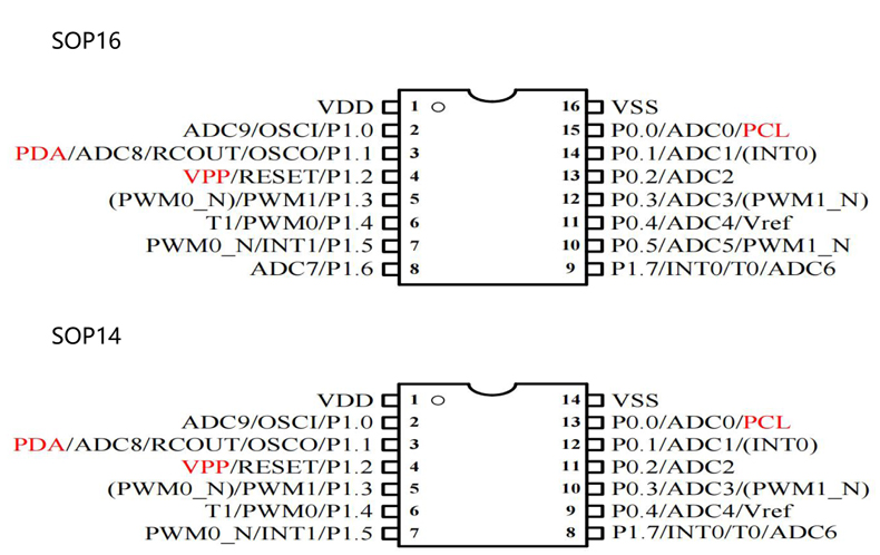
Pin assignment diagram


Copyright © Foshan Angke Electronic Technology Co., Ltd All rights reserved 粤ICP备2023051041号